[Editorial] Packaging with a Punch
![Private: Packaging with a Punch [Editorial]](http://img.global.news.samsung.com/global/wp-content/uploads/2015/04/0414_Inside_Title-Image.jpg)
Samsung’s Semiconductor Series Part 3
Building state-of-the-art semiconductor chips is one thing but making them into the actual square chips we’re familiar with involves a lot of high-tech, too. This process is called packaging, or back-end manufacturing, where chips are essentially sliced off of the silicon wafer, wired up and encased in epoxy for protection.
Let’s say you have a nice order of milkshake that you want to chug down right now. Organic ingredients with crush-ins of your liking, whatever floats your boat. For that, you would need an efficient apparatus (a.k.a. big enough straw) that can deliver a satisfactory flow of sips, preferably an insulated cup that will keep the frothy integrity of the beverage and temperature-resistant nerves that can hold up to the huge amount of milkshake intake against a massive brain freeze. Similar elements and materials are taken into consideration when chips are packaged. Well, okay, it gets way more complicated with semiconductors, but you get the point.
With the amount of data that need to be processed and the speed that is required today, we want to make sure we offer device manufacturers and consumers the total package, in every sense of the phrase, so that the packaging complements the advanced silicon technology inside. This would also determine the size of the final chip. So yes, packaging solutions, even for semiconductor chips, does matter.
Here are some cool examples of Samsung’s approach to this technology.
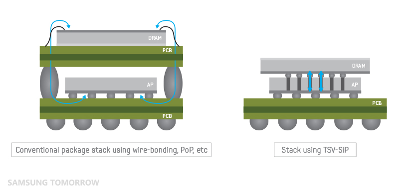
▶ Through Silicon Via (TSV) – We talked about increasing cell density on a single chip for higher capacities but another way to achieve that is to stack individual chip dies in a single package. In doing so, the dies are ground from the back as thin as possible, down to several micrometers, so as to minimize the height of the final product.
Instead of the traditional method of connecting the stacked dies externally, we can now pierce hundreds of tiny holes through DRAM dies and then vertically connect them through the holes, allowing faster data processing with less power consumed. This means that if data were in a building, it can just take the elevator downstairs instead of working its way out to the fire escape. Remember, we’re still working in microscopic scales.
TSV allows approximately twice the speed with about half the power compared to packages using the traditional wire bonding. Again, less space, less power consumption and faster data — another reason our DDR4 DRAM using TSV are so awesome.
![Packaging with a Punch [Editorial]](http://img.global.news.samsung.com/global/wp-content/uploads/2015/04/fig_2.jpg)
▶ ePoP – Sleeker mobile devices mean scarcer space for components, so consolidation is very much desired. As such, even chips with different functions can get bundled together and we’ve seen packages come in forms of eMMC (embedded multi-media card: NAND+controller), eMCP (embedded multi-chip package: DRAM+NAND) or PoP (package on package: AP+DRAM). Samsung’s broad chip portfolio encompassing DRAM, NAND and AP, as well as our advanced packaging capabilities in-house, has naturally given us a huge advantage in this department.
Wonder why there aren’t any packages mentioned above incorporating NAND memory and APs? An active AP can get as hot as 80 to 100℃ whereas NAND would normally get ‘fried’ at that temperature. Because of NAND’s low resistance to heat, it’s been considered that it cannot be in the same package as the AP.
![Packaging with a Punch [Editorial]](http://img.global.news.samsung.com/global/wp-content/uploads/2015/04/fig_3.jpg)
Well, guess what — with an out-of-the-box approach and some new techniques, earlier this year, Samsung was able to introduce the industry’s first ePoP (embedded package on package) memory that can be stacked directly on top of an AP.
Our ePoP memory packs a LPDDR3 DRAM and an eMMC together, dramatically shrinking traditional area configurations by about 40 percent. Thanks to its efficiency and small footprint, Samsung’s ePoP memory is now finding itself on board of wearables as well as high-end mobile devices.
Read more: Samsung Electronics Mass Producing High-Density ePoP Memory for Smartphones
Samsung’s Semiconductor Series
Read Part 1. The Itsy-Bitsy Mighty Chip in a Great Big Digital World
Manager at Device Solutions Division, Samsung Electronics
Insights > Editorials
For any issues related to customer service, please go to
Customer Support page for assistance.
For media inquiries, please click Media Contact to move to the form.