Get the Big Picture: CMOS Image Sensors and ISOCELL

In September 2013, Samsung announced its new advanced pixel technology for the CMOS image sensors (CIS), the ISOCELL technology, which are technology that significantly improves image quality; pretty much any photos you take with your mobile devices. At the MWC 2014, more improved version of the ISCOCELL, 16MP and 13MP. Therefore, we decided to take a moment to understand the technology that allow us to take better photos. Read along and get the big picture of the CMOS image sensor and the new ISOCELL.
CMOS Image Sensor
To understand what the CMOS image sensor is, it is clear that we need to break down the terminology first.
CMOS, complementary metal-oxide semiconductor, is a technology used for building integrated circuits, which are a set of electronic circuits that consist of electrical components connected by a wire which provides an electric current. If you look at it, it pretty much looks a city with many buildings connected by a road, on a chip.

The image sensor is a device that converts light into an electrical signal.
So when we refer generally to the CMOS Image Sensor (CIS), it is an image sensor that is produced with the CMOS technology. More specifically, it’s an image sensor designed as an integrated circuit that contains a number of light-sensitive pixels. CMOS Image Sensor is integrated circuit with array of pixel sensors where each pixel contains a photodetector that senses light and an active amplifier that amplifies the signal.
Therefore, basically, CMOS image sensors (CIS) are the main component that determines the quality of the picture, because they receive light and convert into an electrical signal. Especially when you are talking about any digital imaging device, CMOS image sensors, apart from digital cameras, are extensively used in today’s mobile computing and communication devices, such as smartphones and tablets for photos and videos.
A CIS device is designed as an integrated circuit containing a number of light-sensitive pixels. The self-contained unit also contains circuitry that scans each pixel at fixed intervals providing an electrical pattern of the image falling on the pixels.
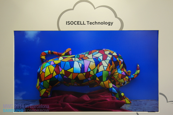
ISOCELL
The key to understanding ISOCELL is the understanding the pixel technology of the image sensor. Previous sensor technology developments focused on improving the light absorption of each pixel. This has progressed pixel technology from FSI (Front Side Illumination) to BSI (Back Side Illumination). Image sensors with FSI have a similar logic to the human eye where images we see are received first through lenses then transported through wires, and then processed into the signal thanks to the photodetector. FSI, just like human eyes, has certain limitations in terms of the light, specifically photons, because the light is processed through a wire (nerves) first.
The BSI technology solves this problem by reversing the whole process. Since the photodetectors receive first and can process more light, it improves the light absorption of each pixel, especially in lowlight situations such as night time.
However, as we constantly demand higher resolution for images, the pixel sizes continue to decrease as well, which eventually brings certain limitations to the BSI technology in improving the image quality. For example, since more lights and colors are being absorbed, then being processed, it could result in noise or color mixing between neighboring pixels.

This is when ISOCELL, the next generation of pixel technology of Samsung comes. Basically, ISOCELL technology forms a physical barrier between neighboring pixels – isolating the pixel. The result, compared to conventional BSI pixels, is that the ISOCELL pixels decrease the crosstalk by approximately 30 percent. It also increases the full well capacity (FWC) by 30% and 20% wider chief ray angle. Samsung is the first to adopt the ISOCELL technology.
This ISOCELL technology gives two key advantages over other image sensor’s technology.

1. Wider, clearer viewing experience without field-of-view(FOV) loss
Even though technology has advanced to a point where we cannot conceive, cameras have not been able to capture the world as we see it. FOV is extremely important in taking high quality photos, because FOV influences the ability of camera to capture the world as human beings see it; generally sees less. The 16MP ISOCELL imager provides a wider, clearer viewing experience to mobile device users by with a 16:9 aspect ratio without field-of-view (FOV) loss.
2. Smart Wide Dynamic Range(WDR)
Samsung’s new 13Mpixel ISOCELL CIS features Smart Wide Dynamic Range (WDR) technology. With a mosaic pattern of multiple exposures, images are then processed with an advanced algorithm for wider dynamic range. Therefore, users can capture the details more accurately in both bright and dark areas even in high contrast lighting conditions. This Smart WDR feature is based on Samsung’s 65nm stacked process, where the pixel array is attached right on top of the logic circuit. Samsung’s 13Mpixel product is sampling now and is scheduled for mass production in the second quarter of 2014.
TAGSMWC 2014
Products > Semiconductors
For any issues related to customer service, please go to
Customer Support page for assistance.
For media inquiries, please click Media Contact to move to the form.