Eight Major Steps to Semiconductor Fabrication, Part 7: The Metal Interconnect
In the last part of our series, we went over the thin-film process in which a semiconductor chip gets its electrical properties. But we need to ensure that these electronic elements are well-connected and “powered” so that the appropriate signals can reach where they need to. This is achieved during the metal interconnect process, which we will discuss in this part of our semiconductor series.
A semiconductor, as you’ve learned before, is a device that can shift between a conductor and a nonconductor, hence its name. In other words, it can allow electricity to flow, or keep it from flowing, whenever necessary.
In order for a TV to turn on, what must be done? It needs to be plugged into a power outlet, of course. The same goes for semiconductors, which is where the metal interconnect process comes into play.
Laying down metal highways that bring semiconductors to life
Utilizing metal’s conductive properties, the metal interconnect process creates metal circuits along the pre-designed patterns. The metal used for semiconductor manufacturing must meet the following requirements:
1. Adhesiveness to the semiconductor substrate (wafer):
The metal needs to easily and strongly adhere to the semiconductor substrate in thin film form.
2. Low electric resistance:
Since the metal circuits deliver the electric current, the substance must have low electric resistance.
3. Thermal and chemical stability:
It is important that the attributes of the metal do not change during the metal interconnect process.
4. Easy formation of patterns:
Regardless of the quality of the metal, it is essential that the material can easily form patterns, especially during the etching process.
5. High reliability:
With the advancement of integrated circuit technology, the metal interconnect material needs to be durable even in minute scale.
6. Manufacturing cost:
Even if the above conditions are met, the cost also has to be suitable for the mass production of semiconductors.
The metals typically used in semiconductor manufacturing that meet the above criteria are aluminum (Al), titanium (Ti) and tungsten (W).
Now, let’s find out how the actual metal interconnect process is carried out.
Popular metals for the interconnect process
Aluminum, one of the main substances used in metal interconnect for semiconductor manufacturing is known to have two merits: great adhesiveness to silicon dioxide and high processability.
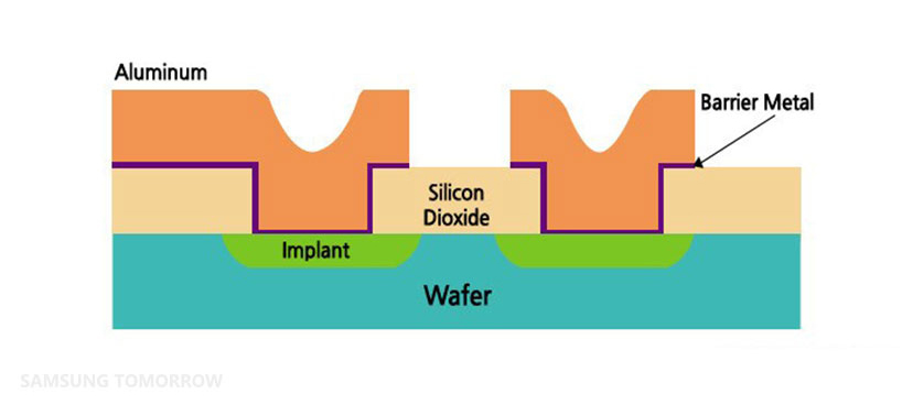
Because aluminum and silicon tend to react with each other, aluminum circuits on semiconductors that are made of silicon may get damaged. To prevent this, a barrier metal is deposited.
Aluminum circuits are created through deposition. When a mass of aluminum is boiled in a decompressed vacuum chamber, the chamber gets filled with aluminum particles. A wafer is then inserted into the vacuum chamber, where the aluminum particles adhere to the wafer and form a thin film. Because aluminum is vaporized and deposited in a high-vacuum environment, this is called the evaporator process. Physical vapor deposition (also known as sputtering) using plasma is also a method widely used today.
A contact is a point where a basic element and a metal interconnect meet. Should the contact be in the form of a narrow tunnel and is difficult to fill, tungsten then comes into play. In such cases, the metal interconnect process is carried out using chemical vapor deposition (CVD) instead of the evaporator process, so as to uniformly deposit the metal as a thin film.
As continued advancements are made in semiconductor technology, semiconductor fabrication processes are also experiencing changes. The metal interconnect process that we discussed today is undergoing a transition from evaporator to chemical vapor deposition so as to better meet the demands of finer design rules. Replacing traditional metals, copper is becoming the material of choice for semiconductor fabrication, thanks to its cost-effectiveness and better conductivity properties.
So there you have it. We have now covered all of the essential processes to design and build the semiconductor circuits on a silicon wafer.
In the next part of our series, we will explore the final step of semiconductor manufacturing, the testing and packaging process, in which silicon wafers are transformed into the individual chips that we see in electronic devices. Stay tuned!
In Korean, http://samsungsemiconstory.com/183.
Products > Semiconductors
For any issues related to customer service, please go to
Customer Support page for assistance.
For media inquiries, please click Media Contact to move to the form.