Eight Major Steps to Semiconductor Fabrication, Part 6: The Addition of Electrical Properties
Did you know that semiconductors are miniature high-rise buildings?
If you get a chance to see a cross section of a semiconductor chip under a high-resolution electron microscope, you will see layer after layer of materials piled up like a skyscraper.
To fabricate such structures, the photolithography and etching processes (which we discussed previously), along with a few others, are repeated a few hundred times until layers of thin film material result in a semiconductor chip.
Today, we will be going over this “thin-film process,” in which a semiconductor chip gets its electrical properties.
Too thin for seein’
The dictionary defines a film thinner than 1 micrometer (μm, one millionth of a meter) as “thin film.” This thickness cannot be manufactured mechanically.
In order for a semiconductor chip to get the desired electrical properties, materials at atomic or molecular levels are densely piled up in the thickness of a thin film. This film is so thin that very elaborate and precise technology is required for it to be deposited evenly on the wafer.
Let’s say we are forming a 1 micrometer-thick film on an 8-inch (200mm) wafer. This would be the equivalent to evenly piling up sand 1mm thick on a schoolyard that is 200m large in diameter. Pretty high-tech, huh?
Deposition: Air-brushing with chemicals
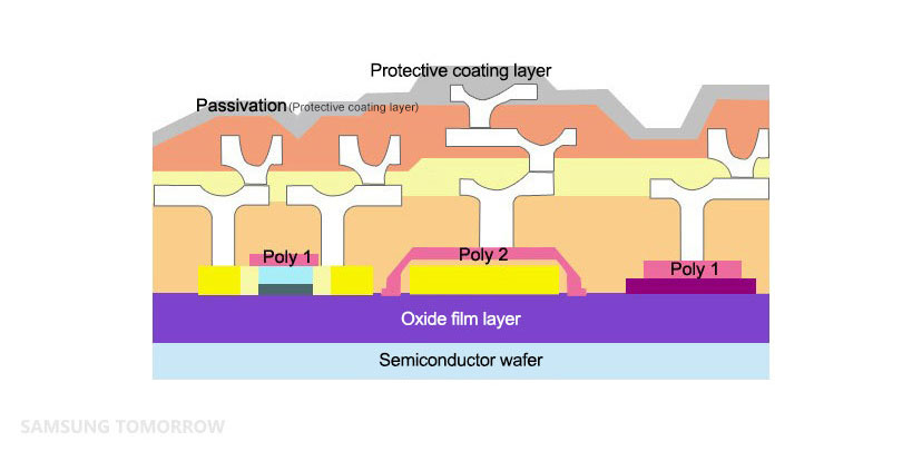
Semiconductor deposition structure
Deposition refers to a series of processes where materials at atomic or molecular levels are deposited on the wafer surface as a thin layer to contain electrical properties.
The deposition methods can be largely divided into physical vapor deposition (PVD) and chemical vapor deposition (CVD).
Physical vapor deposition (PVD) is mainly used for depositing thin metal films and does not involve chemical reactions.
Chemical vapor deposition (CVD) occurs as particles from the chemical reaction of gas are deposited in the form of vapor activated by an external energy source. CVD can be used on conductors and nonconductors, as well as semiconductors.
For this reason, CVD is more commonly used in today’s semiconductor manufacturing processes. The CVD method is further broken down into thermal, plasma-enhanced and optical CVD depending on the source of external energy used. Plasma-enhanced CVD, in particular, yields many benefits as it can be processed at lower temperatures in large volumes while offering greater control over thickness uniformity, making it a preferred method of choice these days.
The thin film fabricated through the deposition process can be categorized into metal (conducting) layers for electrical connections between circuits, and dielectric (insulating) layers that electrically isolate the internal layers or protect them from contaminants.
For semiconductors to develop electric properties, a process of implanting ions on the deposited layer must follow. Ion implantation is the process of implanting electrically charged particles onto a semiconductor surface with circuit patterns. These ions are referred to as “impurities” and include boron (B), phosphorus (P) and arsenic (As). By inserting impurities into the wafer surface in the form of fine gas particles to a desired depth, the silicon wafer acquires its electrical conductivity. (Review the diffusion process to learn more about implanting impurities.)
Today, we looked at how the initially pure, nonconductive silicon wafer is transformed into a semiconducting wafer through the deposition and ion implantation processes. Just how thin and evenly the layer is formed during this deposition process can determine the final chip’s quality.
Stay tuned for the next part of our series, coming next week!
In Korean, http://samsungsemiconstory.tistory.com/172.
Products > Semiconductors
For any issues related to customer service, please go to
Customer Support page for assistance.
For media inquiries, please click Media Contact to move to the form.