Eight Major Steps to Semiconductor Fabrication, Part 1: Creating the Wafer

Although an integrated circuit (IC), also known as a semiconductor chip, may deceive you with its fingernail-sized form factor, it is actually packed with billions of electronic components—transistors, diodes, resistors, and capacitors—which all work together to perform logic operations and store data.
So, what does it take to manufacture this kind of circuit, you ask?
The technology behind engineering an IC goes far beyond the simple assembling of individual components. In fact, microscopic circuit patterns are built on multiple layers of various materials, and only after these steps have been repeated a few hundred times is the chip finally complete.
Today, we are introducing a new series that will walk you through the entire manufacturing process of this advanced device, from the raw material stage to the final testing of the semiconductor chip. The series will consist of eight parts and will be published weekly.
Read on for the first part of the series, which introduces the “canvas” for integrated circuits, otherwise known as the silicon wafer.
What’s a wafer?
A wafer, also called a disc, is a thin, glossy slice of a silicon rod that is cut using specific diameters. Most wafers are made of silicon extracted from sand. The main advantage of using silicon is that it is rich in supply, being the most abundant element in nature, just after oxygen. Its environmentally friendly properties are an added bonus.
Building an ingot, the foundation for wafers
Once silicon is extracted from sand, it needs to be purified before it can be put to use. First, it is heated until it melts into a high-purity liquid then solidified into a silicon rod, or ingot, using common growing methods like the Czochralski (chokh-RAL-skee) process or the Floating Zone process.
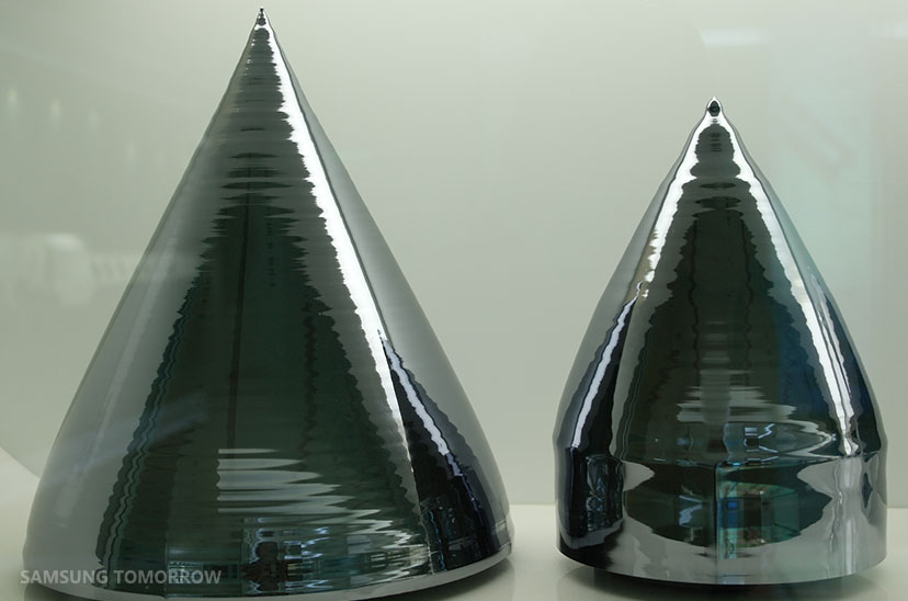
Ends cut off from silicon rods, or ingots
The popular Czochralski method uses a small piece of solid silicon (seed) which is placed in a bath of molten silicon, or polycrystalline silicon, and then slowly pulled in rotation as the liquid grows into a cylindrical ingot. This is why the finished wafers are all round discs.
Giving new meaning to the term “wafer-thin”
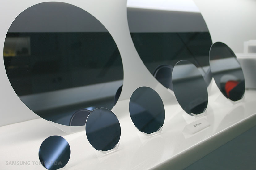
Before it is completely cooled, the cone-shaped ends of the ingot are cut off while the body is sliced into thin wafers of uniform thickness with sharp diamond saw blades. This explains why an ingot’s diameter would ultimately determine the size of a wafer. In the early days of the semiconductor industry, wafers were only three inches in diameter. Since then, wafers have been growing in size, as larger wafers result in more chips and higher productivity. The largest wafer diameter used in semiconductor fabrication today is 12 inches, or 300mm.
Smoothing things out – the lapping and polishing process
Sliced wafers need to be prepped before they are production-ready. Abrasive chemicals and machines polish the uneven surface of the wafer for a mirror-smooth finish. The flawless surface allows the circuit patterns to print better on the wafer surface during the lithography process, which we will cover in a later posting.
Know your wafer
Each part of a finished wafer has a different name and function. Let’s go over them one by one.

1. Chip: a tiny piece of silicon with electronic circuit patterns
2. Scribe Lines: thin, non-functional spaces between the functional pieces, where a saw can safely cut the wafer without damaging the circuits
3. TEG (Test Element Group): a prototype pattern that reveals the actual physical characteristics of a chip (transistors, capacitors, resistors, diodes and circuits) so that it can be tested to see whether it works properly
4. Edge Die: dies (chips) around the edge of a wafer considered production loss; larger wafers would relatively have less chip loss
5. Flat Zone: one edge of a wafer that is cut off flat to help identify the wafer’s orientation and type
This brings us to the end of the first part of the series. Want to know what happens next? Then, stay tuned for Part 2, as Samsung Tomorrow will take you through the disc production stage by discussing the oxidation process of the wafer next week.
In Korean, http://samsungsemiconstory.com/95.
Products > Semiconductors
For any issues related to customer service, please go to
Customer Support page for assistance.
For media inquiries, please click Media Contact to move to the form.